HDI
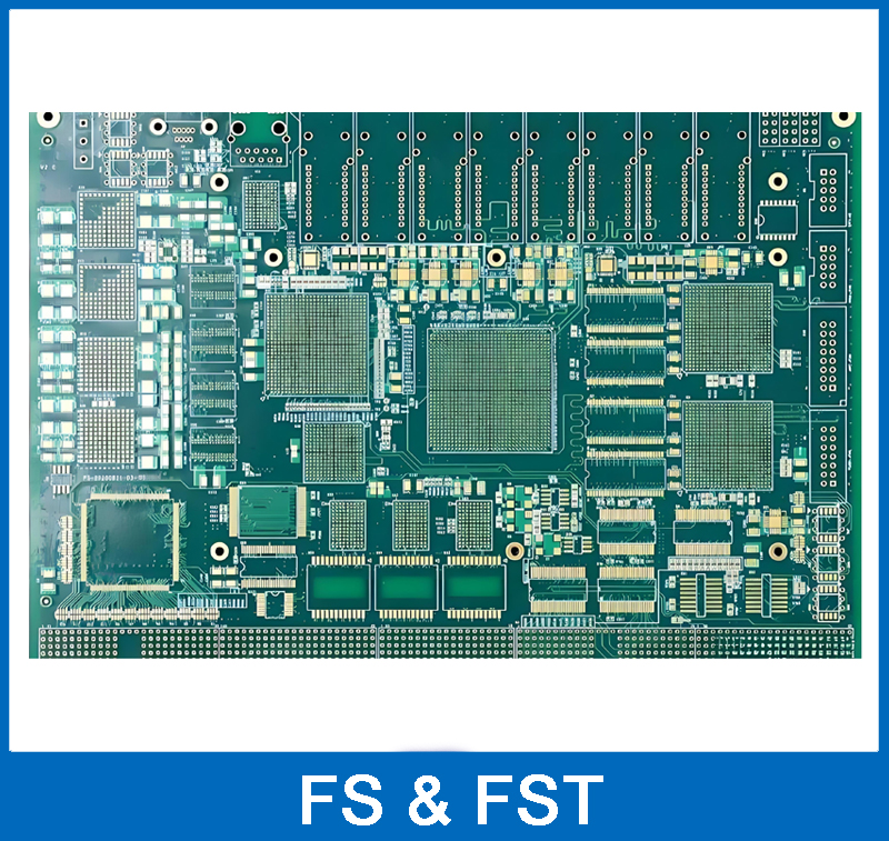
FS & FST Series Precision Multilayer PCB with Impedance Control & High Reliability
1. Product Introduction
The FS & FST Series Precision Multilayer PCB is a high-performance printed circuit board engineered for applications demanding strict impedance control, signal integrity, and long-term operational reliability. Adopting advanced multilayer lamination, precision micro-fabrication, and impedance optimization technologies, this series is designed to support high-speed signal transmission, high-density component integration, and stable operation in harsh industrial, communication, and high-end electronic environments. It fully meets the requirements of high-precision electronic systems for electrical performance stability and mechanical durability.
2. Core Technical Parameters
| Parameter | Specification |
|---|---|
| Number of Layers | 6-32 layers (customizable according to customer requirements) |
| Base Material | FR-4 (Tg 150℃/170℃/180℃), High-Tg FR-4, halogen-free FR-4, high-frequency materials (Rogers/Taconic, optional) |
| Board Thickness | 1.2mm - 8.0mm, tolerance ±0.1mm (customizable) |
| Copper Foil Thickness | Inner layer: 1oz (35μm)/2oz (70μm); Outer layer: 1oz/2oz/3oz (105μm) |
| Minimum Trace Width & Spacing | 3mil (0.075mm) / 3mil (0.075mm) |
| Minimum Drill Diameter | Mechanical drill: 0.15mm; Laser drill (HDI): 0.1mm |
| Aspect Ratio | ≤15:1 (high aspect ratio customization available) |
| Maximum Panel Size | 450mm × 550mm |
3. Impedance Control Performance
- Controlled Impedance Types: Single-ended impedance (50Ω/75Ω), differential impedance (90Ω/100Ω/120Ω)
- Impedance Tolerance: ±8% (Class 3 high-precision standard)
- Impedance Testing: 100% impedance testing via TDR (Time Domain Reflectometer)
- Dielectric Constant Stability: Dk tolerance ±0.05, ensuring consistent impedance performance across the board
4. Manufacturing Process & Surface Treatment
4.1 Lamination & Via Technology
- Lamination process: Vacuum multi-layer lamination, sequential lamination (for HDI blind/buried vias)
- Via types: Through-hole vias, blind vias, buried vias, via-in-pad (VIP) for high-density design
- Plating: Electroless copper + electrolytic copper plating, hole wall copper thickness ≥20μm
4.2 Surface Finish Options
- ENIG (Electroless Nickel Immersion Gold): Ni 3-5μm, Au 0.05-0.1μm (recommended for high reliability)
- Immersion Silver: 0.1-0.3μm (excellent solderability)
- Immersion Tin: 0.8-1.2μm (cost-effective, good thermal stability)
- Lead-free HASL (Hot Air Solder Leveling): RoHS compliant, suitable for mass production
4.3 Solder Mask & Silkscreen
- Solder Mask: Liquid photoimageable solder mask (LPI), colors available in green, black, blue, red
- Silkscreen: White/black ink, minimum character height 0.6mm, clear marking for components and test points
5. Electrical Performance
- Dielectric Strength: ≥50kV/mm (under standard atmospheric conditions)
- Insulation Resistance: ≥1×10¹²Ω (tested at 500V DC)
- Voltage Withstand: No breakdown or flashover at 1500V AC for 60 seconds
- Thermal Conductivity: ≥0.8W/m·K (standard FR-4), ≥2.0W/m·K (high thermal conductivity material)
- Signal Loss: ≤-0.5dB/inch at 10GHz (high-frequency material version)
6. Mechanical & Environmental Reliability
6.1 Mechanical Properties
- Peel Strength: ≥1.2N/mm (copper foil to substrate, IPC-TM-650 2.4.8)
- Bending Strength: ≥400MPa, no cracking under 180° bending test
- Solderability: 100% wettable, no cold solder or non-wetting after 3 times reflow at 260℃
6.2 Environmental Adaptability
- Operating Temperature: -55℃ ~ +150℃ (High-Tg version: -55℃ ~ +175℃)
- Thermal Cycling: Pass 1200 cycles (-40℃ ~ +125℃, 30min/cycle) without delamination, cracking or impedance drift
- Moisture Sensitivity: MSL Level 3, no blistering after 85℃/85%RH/168h humidity test
- Flammability: UL94 V-0, halogen-free version available
7. Quality & Compliance Standards
- Comply with IPC-A-600 Class 2/Class 3 (high-reliability version meets Class 3)
- Comply with IPC-6012 (Qualification and Performance Specification for Rigid Printed Boards)
- RoHS 2.0 (2011/65/EU) and REACH compliant, lead-free and halogen-free options available
- 100% electrical test (flying probe test for high-precision boards, bed of nails test for mass production)
- Pass IPC-TM-650 standard tests for thermal shock, solder resistance, and chemical resistance
8. Application Fields
- High-speed communication equipment (5G base stations, optical transceivers, routers)
- Industrial control systems, PLC, servo drives
- Servers, data center hardware, high-performance computing (HPC)
- Automotive electronics (ADAS, infotainment systems)
- Medical diagnostic equipment, precision instruments
- Aerospace and military electronic modules (customized high-reliability version)
9. Packaging & Storage
- Packaging: Anti-static vacuum packaging + moisture-proof carton, with desiccant and humidity indicator card
- Storage Conditions: Temperature 10-30℃, relative humidity 30-70%RH, avoid direct sunlight, heavy pressure and corrosive gases
- Shelf Life: 12 months (unopened vacuum packaging); 6 months after opening (stored in dry cabinet)
新闻
联系我们
深圳方晟醇和科技有限公司
手机: 86 13428289130
电话: 86 13428289130
邮箱: overseas@fangshengtech.com
地址: 深市宝安区石岩街道塘头社区松白公路西侧宗泰电商科创园B308