PCB生产
PCB Welding:
PCB processing technology up to 64 layers, with minimum trace width/spacing of 2.5/2.5 mil and maximum aspect ratio (board thickness to hole diameter) of 16:1.
- Long & short gold finger processing and high-density circuit precision control, meeting the PCB design requirements of the optoelectronic communication field.
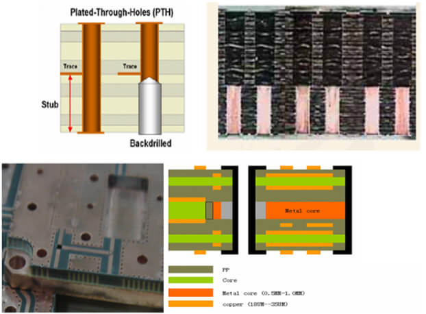
- High-precision back-drilling technology to reduce the equivalent series inductance of vias, ensuring product signal transmission integrity.
- Excellent metal-based and ultra-thick copper manufacturing processes, satisfying the high heat dissipation requirements of power supply products.
- High-precision mechanical and laser depth-control processes to realize multi-step groove structures, meeting the multi-level assembly requirements of products.
- Mature hybrid lamination technology for FR-4 and high-frequency materials, saving material costs for customers while ensuring high-frequency performance.
- Advanced Anti-CAF process, greatly improving the reliability and service life of PCB products.
- Leading embedded capacitor and embedded resistor technologies, significantly enhancing the overall performance of PCBs.
| Maximum Layers | Maximum Panel Size | Minimum Line Width/Space | Maximum Finished Copper Thickness | Minimum Via Annular Ring |
|---|---|---|---|---|
| 40 Layers | 609×889 mm | 2.5/2.5 mil | 6 oz | 3 mil |
| Minimum BGA Pitch | Minimum Finished Hole Diameter | Maximum Aspect Ratio | Minimum Dielectric Thickness | Minimum BGA Pad |
|---|---|---|---|---|
| 0.4 mm | 6 mil (4 mil for Laser Drilled Holes) | 20:1 | 2 mil | 8 mil |
| 2-8L | 10-18L | 20-30L | 20-30L |
|---|---|---|---|
| 4-8 Days | 10-14 Days | 15-18 Days | 18-22 Days |
Strict Quality Management for PCBs
1.UL Certification;2.ISO 9001:2008 Quality System Certification;
3.ISO/TS 16949:2009 System Certification;
4.GJB 9001B Military Standard System Certification;
5.Compliance with enterprise standards of Huawei, ZTE, etc.;
6.Customized PCB processing strictly managed in accordance with IPC‑A‑600 Class 1/2/3, military standards, customer specifications and internal enterprise standards;
7.Strict customer information confidentiality management system.
Advanced Processing and Testing Equipment
1.Orbotech AOI (Automatic Optical Inspection) machines imported from Israel, used for inspecting increasingly fine circuit board products.2.High-precision impedance testers imported from the U.S., which meet the impedance testing requirements of PCB products.
3.Advanced plasma treatment equipment, used for desmearing processes on hole walls of high-frequency materials such as PTFE and ceramic-filled substrates.
4.END CNC drilling machines imported from Taiwan, used for back drilling and controlled-depth hole processing.
5.Orbotech LDI (Laser Direct Imaging) machines imported from Israel, used for high-precision circuit pattern transfer.
6.END CNC routing machines imported from Taiwan, used for controlled-depth milling of PCBs with stepped groove structures.
7.BURKLE presses imported from Germany, used for the lamination process of high-layer PCBs.
8.Vacuum resin plugging machines, used for via-in-pad processes on BGA pads of high-precision fine-line PCBs.
9.A full range of reliability testing equipment, including ion contamination testers, peel strength testers, copper thickness testers, 2D measuring machines, gold thickness testers, etc., to strongly ensure the quality of customers’ PCB products.

新闻
联系我们
Contact: 深圳方晟醇和科技有限公司
86 13428289130: 86 13428289130
Tel: 86 13428289130
E-mail: overseas@fangshengtech.com
Add: 深市宝安区石岩街道塘头社区松白公路西侧宗泰电商科创园B308