The Microscopic Cornerstone of the Internet of Everything: The In-depth Connection Between IoT Devices and Precision Manufacturing
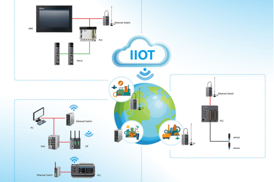
When a smartwatch accurately monitors heart rate, when industrial sensors transmit data from kilometer-deep wells, and when urban streetlights automatically adjust brightness based on pedestrian flow—behind these scenarios lies a massive neural network composed of tens of billions of IoT devices. The essence of the Internet of Things (IoT) is not a single technological revolution, but the digitization of the physical world through a three-layer collaborative architecture: the Perception Layer, like peripheral nerves, collects signals such as temperature, vibration, and light intensity via micro-electro-mechanical sensors; the Transport Layer serves as the transmission path, with 5G and LPWAN technologies enabling millisecond-level data upload; the Application Layer, like a cloud-based brain, optimizes decisions through AI algorithms. According to Statista, a global market research firm, 75 billion IoT devices will be in operation worldwide by 2025, with China accounting for over 35% of the market. Smart homes, industrial monitoring, and smart cities constitute the three major application pillars.

The Morphological Evolution of IoT Devices
IoT devices have broken through the morphological boundaries of traditional electronic products. In the consumer sector, TWS earbuds implement head-tracking spatial audio through six-axis gyroscopes, while the PPG photoelectric sensor in medical-grade smartwatches can capture 0.1mm blood vessel micro-movements with a heart rate monitoring accuracy of ±2 bpm. In industrial scenarios, vibration sensors can identify 0.01mm-level mechanical displacement, and predictive maintenance systems have pushed the accuracy of equipment failure early warning beyond 90%. Smart cities rely on high-precision metering terminals—smart electricity meters achieve ±0.5% power measurement accuracy, and air quality monitoring stations have a PM2.5 resolution of 1μg/m³. Even more miniaturized MEMS sensors, only 2mm² in size, can withstand 200g impact, while ultra-high-frequency RFID tags accurately identify cargo information from 10 meters away.
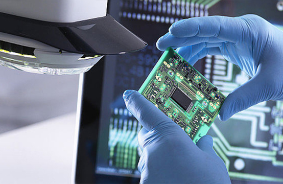
The physical carrier supporting these functions is precisely the PCBA (Printed Circuit Board Assembly). A matchbox-sized PCBA for industrial sensors may integrate more than 200 components, and its manufacturing process can be called a precision engineering on the microscopic scale.
Three Key Challenges in PCBA Manufacturing
Miniaturization
The continuous miniaturization of component sizes has spawned new process standards: 01005 packaged components (0.4×0.2mm) require placement machines with a positioning accuracy of ±25μm, equivalent to 1/3 the diameter of a human hair; laser-cut stencils control the fluctuation of solder paste printing thickness within ±15μm, as thickness deviations exceeding this range will cause cold solder joints in microcapacitors; High-Density Interconnect (HDI) boards adopt an 8-layer blind and buried via design, and the 40μm line width requires strict impedance tolerance control within ±5% to avoid high-speed signal reflection. For Ball Grid Array (BGA) chips, X-ray inspection must ensure the solder void rate is below 15%, and the slope error of the reflow oven temperature zone curve shall not exceed ±2℃/s; otherwise, the imbalance of molten tin surface tension will cause bridging.
Extreme Environments
Industrial IoT devices often face harsh operating conditions: oilfield sensors need to work continuously for ten years at a temperature difference of -55℃~125℃. Their PCBs use ceramic substrates (with a thermal expansion coefficient of 4.5ppm/℃) to match the material characteristics of chips, and reliability is verified through 200 thermal cycle tests; the vibration test standard for automotive equipment is as high as 15Grms (equivalent to 1/3 of the acceleration of rocket launch), requiring dispensing and reinforcement at the four corners of QFN chips; devices deployed in coastal cities rely on polyurethane-silicone composite three-proof coatings, with salt spray resistance exceeding 2000 hours. Long-term operation also requires the selection of solid-state capacitors (with a lifespan of over 50,000 hours at 85℃) and gold bonding wires to completely avoid the risk of electrochemical migration.
Signal Integrity
The RF performance of 5G communication modules directly depends on circuit design: hybrid PCBs combine Rogers RO4350B high-frequency materials with conventional FR-4, resulting in a dielectric loss of less than 0.0037 in the 10GHz band; RF traces strictly follow the 3W rule (line spacing ≥3 times the line width) and implement full ground shielding. The power supply network uses a 2oz thick copper layer combined with stepped decoupling capacitors (10μF tantalum capacitors + 0.1μF ceramic capacitor arrays) to suppress the power supply ripple of the core chip within 50mV.
Nano-level Control in the Manufacturing Chain
IoT PCBA manufacturing has formed a full-process quality closed loop: in the design phase, thermal simulation software locates overheating areas, and DFM rules mandate that pad gaps be larger than 0.1mm; in the production phase, solder paste printers are equipped with 3D inspection tools (SPI), and strict control of thickness tolerance within ±15μm reduces the cold solder joint probability by 83%; after placement, the AOI system achieves 0.01mm-level component positioning using multi-spectral imaging (450-850nm band); reflow soldering adopts Sn96.5/Ag3/Cu0.5 eutectic solder paste, and the temperature fluctuation in the 217℃ melting point range must be less than ±2℃. In the final testing phase, the Highly Accelerated Life Test (HALT) stimulates potential defects through rapid temperature changes of -55℃~125℃, reducing the after-sales failure rate of mass-produced equipment to 0.12 parts per million.
The Breakthrough Path of "Made in China"
Facing the global demand for IoT devices with an annual growth rate of 12%, Chinese manufacturing is achieving key technological breakthroughs: SiP (System-in-Package) technology stacks sensors, MCUs, and wireless modules in 3D, reducing volume by 60%; glass substrates, with an ultra-low thermal expansion coefficient of 0.5ppm/℃, pave the way for 2μm line width mass production in 2025; green manufacturing processes adopt lead-free solder and water-based cleaning agents, reducing volatile organic compound emissions by 90%. According to statistics from the China Semiconductor Industry Association, the localization rate of IoT chips in China reached 28% in 2023 and is expected to exceed 35% by 2025—meaning that among every three IoT devices made in China, one will be equipped with an independently designed "heart".
Summary
The evolutionary history of IoT devices is essentially a symphony of nano-scale materials and micro-scale processes. When an industrial sensor operates continuously for 100,000 hours in an Arctic oilfield, and when a medical chip precisely regulates insulin injection for diabetic patients—behind these miracles are countless engineers building lifelines on the scale of 0.01 millimeters. As China's semiconductor ecosystem matures, smart devices born on this land are redefining the precision and temperature of the Internet of Everything.